Ohm (symbol Ω) is the electrical unit of resistance

Ohm (symbol Ω) is the electrical unit of resistance

Ohm (Ω)

Ohm (symbol Ω) is the electrical unit of resistance.
The Ohm unit was named after George Simon Ohm.
1Ω = 1V / 1A = 1J ⋅ 1s / 1C2

Table of resistance values of Ohm

namesymbolconversionexample
milli-ohmmΩ1mΩ = 10-3ΩR0 = 10mΩ
ohmΩ
-
R1 = 10Ω
kilo-ohmkΩ1kΩ = 103ΩR2 = 2kΩ
mega-ohmMΩ1MΩ = 106ΩR3 = 5MΩ

Ohmmeter

Ohmmeter is a measurement device that measures resistance.

Download Bios bin file Laptop Acer Aspire 722


File Name : Bios File Acer Aspire 722.zip
Size : 962 KB

Download Bios bin file Laptop Acer Aspire ES1-432


File Name : Bios File Acer Aspire ES1-432.zip
Size : 4 MB

Download Bios bin file Laptop Acer Aspire E5-411


File Name : Bios File Acer Aspire E5-411.zip
Size : 2 MB
Classification and Different Types of Transistors | BJT, FET, NPN, PNP

Classification and Different Types of Transistors | BJT, FET, NPN, PNP

In this tutorial, we will learn about the classification and different Types of Transistors. The Transistor became an essential component in modern electronics and we cannot imagine the World without Transistors. 

Introduction

Transistor is a semiconductor device which is used to amplify the signals as well as in switching circuits. Generally transistor is made of solid material which contains three terminals such as emitter (E), Base (B) and Collector (C) for connections with other components in the circuit. Some transistors contains fourth terminal also i.e. substrate (S). Transistor is one of the active components.
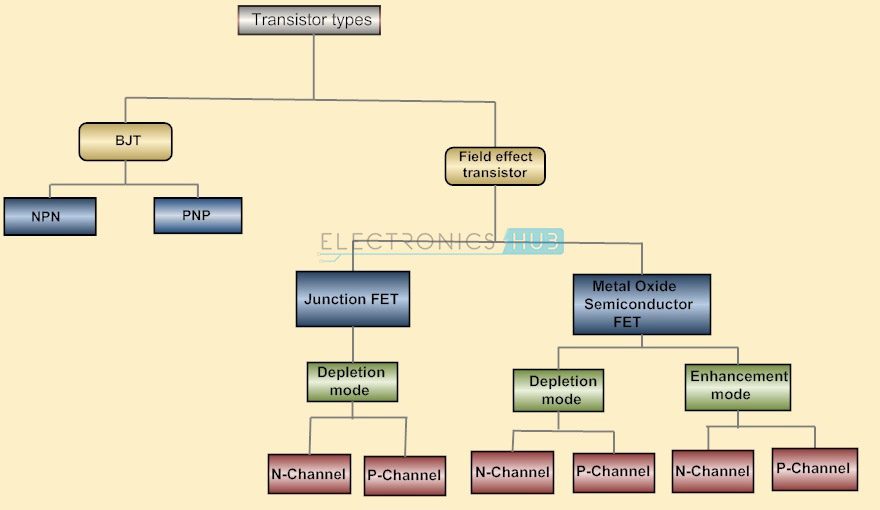
From the time of first transistor invention to present days the transistors are classified into different types depending on either construction or operation, they are explained using tree diagram as below.

Transistor Tree Diagram

1.Transistor tree
The transistors classification can be understood by observing the above tree diagram. Transistors are basically classified into two types; they are Bipolar Junction Transistors (BJT) and Field Effect Transistors (FET). The BJTs are again classified into NPN and PNP transistors. The FET transistors are classified into JFET and MOSFET.
Junction FET transistors are classified into N-channel JFET and P-channel JFET depending on their function. MOSFET transistors are classified into Depletion mode and Enhancement mode. Again depletion and enhancement mode transistors are classified into N-channel JFET and P-channel.
Nowadays, the vacuum tubes are replaced with transistors because the transistors have more benefits over vacuum tubes. Transistors are small in size and it requires low voltage for operation and also it has low power dissipation. Due to these reasons the transistor is used in many applications such as amplifiers, switching circuits, oscillators and also in almost all electronic circuits.

Types of Transistors

Transistor is the proper arrangement of different semiconductor materials. General semiconductor materials used for transistor are silicon, germanium, and gallium-arsenide. Basically the transistors are classified depending on their structure. Each type of transistors has their own characteristics, advantages and disadvantages.
Some transistors are designed primarily for switching purpose, other side some are designed for amplification purpose and some transistors are designed for both amplification and switching purposes. Depending on the structure the transistors are classified into BJT and FET.

Junction Transistors

Junction transistor is generally called as Bipolar Junction Transistor (BJT). The BJT transistors have three terminals named emitter (E), Base (B), Collector (C). The name itself indicates that it has two junctions between p-type and n-type semiconductors. The BJT transistors are classified in to NPN and PNP transistors depending on the construction.
Unlike FET transistors, the BJT transistors are current-controlled devices. If small amount of current flows through the base of a BJT transistor then it causes to flow large current from emitter to collector. The BJT transistors have low input impedance and it causes to flow large current through the transistor.
The BJT transistors are only the transistors which are turned ON by the input current which is given to the base. Bipolar junction transistors can operate in three regions, they are
  • Cut-off Region: Here the transistor is in ‘OFF’ state i.e the current flowing through the transistor is zero.
  • Active Region: Here the transistor acts as an amplifier.
  • Saturation Region: Here the transistor is in fully ‘ON’ state and also works as a closed switch.

NPN Transistor

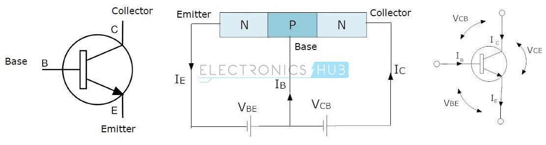
NPN is one of the two types of Bipolar Junction Transistors (BJT). The NPN transistor consists of two n-type semiconductor materials and they are separated by a thin layer of p-type semiconductor. Here the majority charge carriers are electrons and holes are the minority charge carriers. The flowing of electrons from emitter to collector forms the current flow in the transistor through the base terminal.
A small amount of current at base terminal causes to flow large amount current from emitter to collector. Nowadays the generally used bipolar transistor is NPN transistor, because the mobility of electrons is greater than mobility of holes. The standard equation for the currents flowing in the transistor is
IE = IB + IC
The symbols and structure for NPN transistors are given below.
2. NPN transistor symbols

PNP Transistor

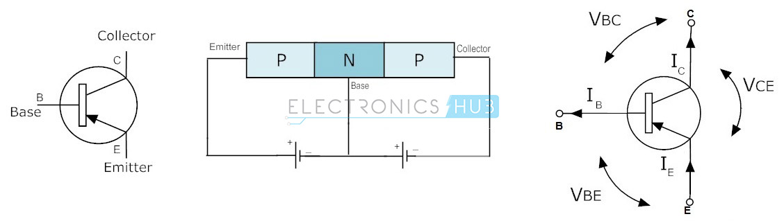
The PNP is another type of Bipolar Junction Transistors (BJT). The PNP transistors contain two p-type semiconductor materials and are separated by a thin layer of n-type semiconductor. The majority charge carriers in the PNP transistors are holes and electrons are minority charge carriers. The arrow in the emitter terminal of transistor indicates the flow of conventional current. In PNP transistor the current flows from Emitter to Collector.
The PNP transistor is ON when the base terminal is pulled to LOW with respect to emitter. The symbol and structure for PNP transistor is shown below.
3. Circuit symbol and structure for PNP

FET (Field Effect Transistor)

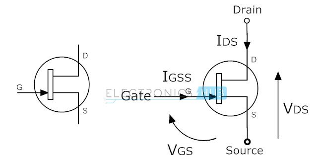
The Field-Effect-Transistor (FET) is another transistors type. Basically the FET transistors have three terminals they are gate (G), Drain (D) and Source (S). FET transistors are classified into Junction Field Effect transistors (JFET) and Insulated Gate FET (IG-FET) or MOSFET transistors. For the connections in the circuit we also consider fourth terminal called base or substrate. The FET transistors have control on the size and shape of a channel between source and drain which is created by applied voltage. The FET transistors are uni-polar transistors because they perform single channel operation where as BJT transistors are bipolar junction transistors. The FET transistors have high current gain than BJT transistors.

JFET (Junction-Field Effect Transistor)

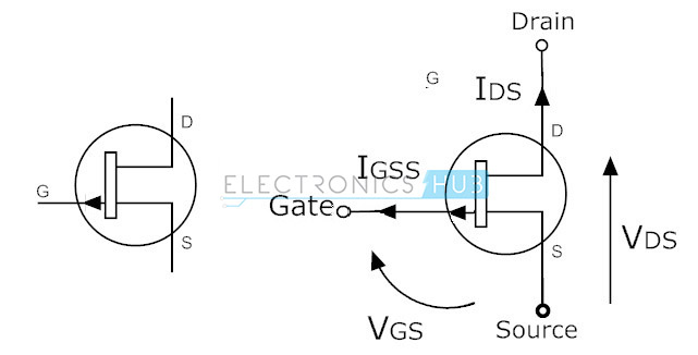
The Junction-Field-Effect transistor (JFET) is an earliest and simple type of FET transistors. These JFETs are used as switches, amplifiers and resistors. This transistor is a voltage controlled device. It doesn’t need any biasing current. The voltage applied between gate and source controls the flow of electric current between source and drain of a transistor. The JFET transistors are available in both N-channel and P-channel types.

N-Channel JFET

In N-channel JFET the current flow is due to the electrons. When voltage is applied between gate and source, a channel is formed between source and drain for current flow. This channel is called N-channel. Nowadays N-channel JFET transistor is most preferable type than P-channel JFET. The symbols for N-channel JFET transistor are given below.
4. N-channel jfet symbols

P-Channel JFET

In this JFET transistor the current flow is because of holes. The channel between source and drain is called P-channel. The symbols for P-channel JFET transistors are given below. Here arrow marks indicates the direction of current flow.
5. p-channel jfet symbols

MOSFET

Metal-Oxide-Semiconductor Field Effect Transistor (MOSFET) is most useful type of among all transistors. The name itself indicates that it contains metal gate terminal. The MOSFET has four terminals drain, source, gate and body or substrate (B). MOSFET has many advantages over BJT and JFET, mainly it offer high input impedance and low output impedance. It is used in low power circuits mainly in chip designing technologies.
The MOSFET transistors are available in depletion and enhancement types. Further the depletion and enhancement types are classified into N-channel and P-channel types.

N-Channel MOSFET

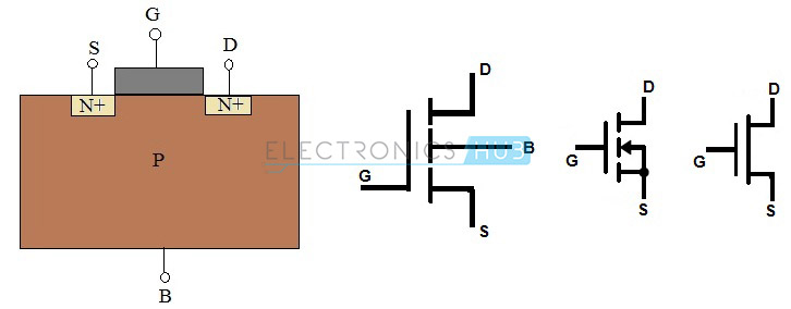
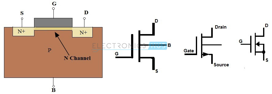
The MOSFET having N-channel region between source and drain is called N-channel MOSFET. Here the source and gate terminals are heavily doped with n-type materials and substrate is doped with p-type semiconductor material. Here the current flow between source and drain is because of electrons. The gate voltage controls the current flow in the circuit. N-channel MOSFET is most preferable than P-channel MOSFET because the mobility of electrons is high than mobility of holes. The symbols for N-channel MOSFET transistors are given below.
6 enhancement mode
6 .Depletion mode

P- Channel MOSFET

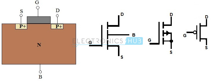
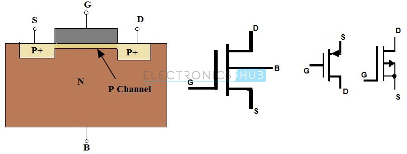
The MOSFET having P-channel region between source and drain is called as P-channel MOSFET. Here the source and drain terminals are heavily doped with P-type material and the substrate is doped with N-type material. The current flow between source and drain is because of holes concentration. The applied voltage at gate will controls the flow of current through channel region. The symbols for P-channel MOSFET transistors in depletion and enhancement types are given below.
7 .p-channel enhancement mode
7. P-Channel depletion mode

Transistors Based on Function

Transistors are also classified depending on the functions that mean what the transistors do. Different types of transistors based on their function are explained below.

Small Signal Transistors

The basic function of small signal transistors is to amplify small signals even these transistors are used for switching purpose. Small signal transistors are available in market in the form of NPN and PNP transistors. We can see some value on the body of small signal transistor this value indicates hFE of transistor.
Depending on this hFE value we can understand the capacity of transistor to amplify the signal. The hFE values are present within the range of 10 to 500. The collector current value of these transistors is 80 to 600mA. This type of transistors operates with the frequency range of 1 to 300MHz. The name of the transistor itself indicates that these transistors amplify small signals which use small voltages and currents, such as few milli volts and milli amperes of current.
Small-signal-transistor
Resource link: learningaboutelectronics.com/images/Small-signal-transistor.png
Small signal transistors are used in almost all types of electronic equipments and also these transistors are used in several applications, some of them are ON or OFF switches for general use, LED diode driver, Relay driver, Audio mute function, Timer circuits, Infrared diode amplifier, Bias supply circuits etc.

Small Switching Transistors

Small switching transistors are the transistors which are primarily used for switching after that also used for amplification. Like small signal transistors, small switching transistors are also available in the form of NPN and PNP and these type of transistors are also have hFE values. The hFE value range for these transistors is from 10 to 200. At hFE value 200 the transistors are not good amplifiers even though they act as better switches. The collector current values ranges from 10 to 1000mA. These transistors are used mostly in switching applications.
Small-switching-transistorResource link: learningaboutelectronics.com/images/Small-switching-transistor.png

Power Transistors

The transistors which are used in the high power amplifiers and power supplies are called as “power amplifiers”. The collector terminal of this transistor is connected to the base of a metal device and this structure acts as heat sink which dissipates excess power for the applications.
These types of transistors are available in the form of NPN, PNP and Darlington transistors. Here the collector current values range from 1 to 100A. The operating frequency range from 1 to 100MHz. The power values of these transistors are range from 10 to 300W. The name of the transistor itself indicates that the power transistors are used in the applications where high power, high voltage and high current are required.
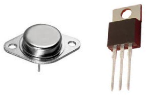
Power-transistorsResource link: learningaboutelectronics.com/images/Power-transistors.png

High Frequency Transistors

High frequency transistors are used for small signals which operate at high frequencies and these are used in high speed switching applications. High frequency transistors are also called as RF Transistors. These transistors have maximum frequency values of about 2000MHz. The collector current (IC) value ranges from 10 to 600mA. These types of transistors are also available in the form of NPN and PNP. These are mainly used in the applications of high frequency signals and also this transistors must be ON or OFF at high speeds only. These transistors are used in HF, VHF, UHF, CATV and MATV oscillator and amplifier circuits.
High-frequency-transistors
Resource link: learningabouelectronics.com/images/High-frequency-transistors.jpg

Photo Transistor

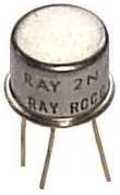
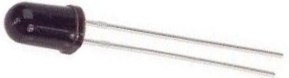
Photo transistors are the transistors which operate depending on the light that means these transistors are light sensitive. The general photo transistor is nothing but a bipolar transistor which contains light sensitive area instead of base terminal. The photo transistors have only 2 terminals instead of general 3 terminals. The transistor operates depending on the light. When the light sensitive area is dark then no current flows in transistor i.e. transistor is in OFF state.
Phototransistors
Resource link: learningaboutelectronics.com/images/Phototransistors.jpg
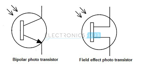
8. photo transistors
When light sensitive area is exposed to light then a small amount of current generates at base terminal and it causes to flow large current from collector to emitter. The photo transistors are available in both BJT and FET transistor types. These are named as photo-BJTs and photo-FETs.
Unlike photo-BJTs, the photo-FETs are generating gate current by using light which controls the current flow between drain and source terminals. Photo-FETs are more sensitive to light than photo-BJTs. The symbols for photo-BJT and photo-FETs are shown above.

Unijunction Transistors:

Unijunction-transistor
Resource link: learningaboutelectronics.com/images/Unijunction-transistor.png
9.unijunction transistor
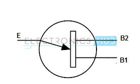
Unijunction transistors are used only as electrically controlled switches. These transistors do not contain any amplification characteristics because of their design. These are generally three lead transistors. Now we see the operation of unijunction transistor. If there is no potential difference between emitter and any one of the base terminals (B1 or B2) then a small amount of current flows between B1 and B2.
If sufficient amount of voltage is applied to the emitter terminal then high current generates at emitter terminal and it adds to small current between B1 and B2, then it causes to flow large current in the transistor. Here the emitter current is the primary current source for total current in the transistor. The current between the terminals B1 and B2 is very small, due to this reason these transistors are not suitable for amplification purpose.

Download Bios bin file Laptop Acer Aspire E1-431


File Name : Bios File Acer Aspire E1-431.zip
Size : 842 KB

Download Bios bin file Laptop Acer Aspire 4732


File Name : Bios File Acer Aspire 4732.zip
Size : 842 KB
Superconductivity

Superconductivity

Conductors lose all of their electrical resistance when cooled to super-low temperatures (near absolute zero, about -273° Celsius). It must be understood that superconductivity is not merely an extrapolation of most conductors’ tendency to gradually lose resistance with decreasing temperature; rather, it is a sudden, quantum leap in resistivity from finite to nothing. A superconducting material has absolutely zero electrical resistance, not just some small amount.
Superconductivity was first discovered by H. Kamerlingh Onnes at the University of Leiden, Netherlands, in 1911. Just three years earlier, in 1908, Onnes had developed a method of liquefying helium gas, which provided a medium with which to supercool experimental objects to just a few degrees above absolute zero. Deciding to investigate changes in electrical resistance of mercury when cooled to this low of a temperature, he discovered that its resistance dropped to nothing just below the boiling point of helium.
There is some debate over exactly how and why superconducting materials superconduct. One theory holds that electrons group together and travel in pairs (called Cooper pairs) within a superconductor rather than travel independently, and that has something to do with their frictionless flow. Interestingly enough, another phenomenon of super-cold temperatures, superfluidity, happens with certain liquids (especially liquid helium), resulting in frictionless flow of molecules.
Superconductivity promises extraordinary capabilities for electric circuits. If conductor resistance could be eliminated entirely, there would be no power losses or inefficiencies in electric power systems due to stray resistances. Electric motors could be made almost perfectly (100%) efficient. Components such as capacitors and inductors, whose ideal characteristics are normally spoiled by inherent wire resistances, could be made ideal in a practical sense. Already, some practical superconducting conductors, motors, and capacitors have been developed, but their use at this present time is limited due to the practical problems intrinsic to maintaining super-cold temperatures.
The threshold temperature for a superconductor to switch from normal conduction to superconductivity is called the transition temperature. Transition temperatures for “classic” superconductors are in the cryogenic range (near absolute zero), but much progress has been made in developing “high-temperature” superconductors which superconduct at warmer temperatures. One type is a ceramic mixture of yttrium, barium, copper, and oxygen which transitions at a relatively balmy -160° Celsius. Ideally, a superconductor should be able to operate within the range of ambient temperatures, or at least within the range of inexpensive refrigeration equipment.
The critical temperatures for a few common substances are shown here in this table. Temperatures are given in kelvins, which has the same incremental span as degrees Celsius (an increase or decrease of 1 kelvin is the same amount of temperature change as 1° Celsius), only offset so that 0 K is absolute zero. This way, we don’t have to deal with a lot of negative figures.
MaterialElement/AlloyCritical temp.(K)
AluminumElement1.20
CadmiumElement0.56
LeadElement7.2
MercuryElement4.16
NiobiumElement8.70
ThoriumElement1.37
TinElement3.72
TitaniumElement0.39
UraniumElement1.0
ZincElement0.91
Niobium/TinAlloy18.1
Cupric sulphideCompound1.6
Superconducting materials also interact in interesting ways with magnetic fields. While in the superconducting state, a superconducting material will tend to exclude all magnetic fields, a phenomenon known as the Meissner effect. However, if the magnetic field strength intensifies beyond a critical level, the superconducting material will be rendered non-superconductive. In other words, superconducting materials will lose their superconductivity (no matter how cold you make them) if exposed to too strong of a magnetic field. In fact, the presence of any magnetic field tends to lower the critical temperature of any superconducting material: the more magnetic field present, the colder you have to make the material before it will superconduct.
This is another practical limitation to superconductors in circuit design, since electric current through any conductor produces a magnetic field. Even though a superconducting wire would have zero resistance to oppose current, there will still be a limit of how much current could practically go through that wire due to its critical magnetic field limit.
There are already a few industrial applications of superconductors, especially since the recent (1987) advent of the yttrium-barium-copper-oxygen ceramic, which only requires liquid nitrogen to cool, as opposed to liquid helium. It is even possible to order superconductivity kits from educational suppliers which can be operated in high school labs (liquid nitrogen not included). Typically, these kits exhibit superconductivity by the Meissner effect, suspending a tiny magnet in mid-air over a superconducting disk cooled by a bath of liquid nitrogen.
The zero resistance offered by superconducting circuits leads to unique consequences. In a superconducting short-circuit, it is possible to maintain large currents indefinitely with zero applied voltage!
rings of superconducting material
Rings of superconducting material have been experimentally proven to sustain continuous current for years with no applied voltage. So far as anyone knows, there is no theoretical time limit to how long an unaided current could be sustained in a superconducting circuit. If you’re thinking this appears to be a form of perpetual motion, you’re correct! Contrary to popular belief, there is no law of physics prohibiting perpetual motion; rather, the prohibition stands against any machine or system generating more energy than it consumes (what would be referred to as an over-unity device). At best, all a perpetual motion machine (like the superconducting ring) would be good for is to store energy, not generate it freely!
Superconductors also offer some strange possibilities having nothing to do with Ohm’s Law. One such possibility is the construction of a device called a Josephson Junction, which acts as a relay of sorts, controlling one current with another current (with no moving parts, of course). The small size and fast switching time of Josephson Junctions may lead to new computer circuit designs: an alternative to using semiconductor transistors.
REVIEW:
  • Superconductors are materials which have absolutely zero electrical resistance.
  • All presently known superconductive materials need to be cooled far below ambient temperature to superconduct. The maximum temperature at which they do so is called the transition temperature.
From Electric to Electronic

From Electric to Electronic

Introduction

This third volume of the book series Lessons In Electric Circuits makes a departure from the former two in that the transition between electric circuits and electronic circuits is formally crossed. Electric circuits are connections of conductive wires and other devices whereby the uniform flow of electric charges occurs. Electronic circuits add a new dimension to electric circuits in that some means of control is exerted over the flow of electric charges by another electrical signal, either a voltage or a current.

Electronic Circuits

In and of itself, the control of electric charge flow is nothing new to the student of electric circuits. Switches control the flow of electric charges, as do potentiometers, especially when connected as variable resistors (rheostats). Neither the switch nor the potentiometer should be new to your experience by this point in your study. The threshold marking the transition from electric to electronic, then, is defined by how the flow of electric charges is controlled rather than whether or not any form of control exists in a circuit. Switches and rheostats control the flow of electric charges according to the positioning of a mechanical device, which is actuated by some physical force external to the circuit. In electronics, however, we are dealing with special devices able to control the flow of electric charges according to another flow of electric charges, or by the application of a static voltage. In other words, in an electronic circuit, electricity is able to control electricity.

History of the Modern Electronics Era

Thomas Edison

The historic precursor to the modern electronics era was invented by Thomas Edison in 1880 while developing the electric incandescent lamp. Edison found that a small current passed from the heated lamp filament to a metal plate mounted inside the vacuum envelope. (Figure below (a)) Today this is known as the “Edison effect”. Note that the battery is only necessary to heat the filament. Electrons would still flow if a non-electrical heat source was used.
Edison effect, Fleming valve or vacuum diode, DeForest audion triode vacuum tube amplifier.

Vacuum Diode

By 1904 Marconi Wireless Company adviser John Flemming found that an externally applied current (plate battery) only passed in one direction from filament to plate (Figure above (b)), but not the reverse direction (not shown). This invention was the vacuum diode, used to convert alternating currents to DC. The addition of a third electrode by Lee DeForest (Figure above (c)) allowed a small signal to control the larger electron flow from filament to plate.

Audion Tube

Historically, the era of electronics began with the invention of the Audion tube, a device controlling the flow of an electron stream through a vacuum by the application of a small voltage between two metal structures within the tube. A more detailed summary of so-called electron tube or vacuum tube technology is available in the last chapter of this volume for those who are interested.

Transistor

Electronics technology experienced a revolution in 1948 with the invention of the transistor. This tiny device achieved approximately the same effect as the Audion tube, but in a vastly smaller amount of space and with less material. Transistors control the flow of electric charges through solid semiconductor substances rather than through a vacuum, and so transistor technology is often referred to as solid-state electronics.

Conductors, Insulators, and Electron Flow

The electrons of different types of atoms have different degrees of freedom to move around. With some types of materials, such as metals, the outermost electrons in the atoms are so loosely bound that they chaotically move in the space between the atoms of that material by nothing more than the influence of room-temperature heat energy. Because these virtually unbound electrons are free to leave their respective atoms and float around in the space between adjacent atoms, they are often called free electrons.


Conductors vs Insulators

In other types of materials such as glass, the atoms’ electrons have very little freedom to move around. While external forces such as physical rubbing can force some of these electrons to leave their respective atoms and transfer to the atoms of another material, they do not move between atoms within that material very easily.
This relative mobility of electrons within a material is known as electric conductivity. Conductivity is determined by the types of atoms in a material (the number of protons in each atom’s nucleus determines its chemical identity) and how the atoms are linked together with one another. Materials with high electron mobility (many free electrons) are called conductors, while materials with low electron mobility (few or no free electrons) are called insulators. Here are a few common examples of conductors and insulators:
  • Conductors
  • silver
  • copper
  • gold
  • aluminum
  • iron
  • steel
  • brass
  • bronze
  • mercury
  • graphite
  • dirty water
  • concrete
  • Insulators
  • glass
  • rubber
  • oil
  • asphalt
  • fiberglass
  • porcelain
  • ceramic
  • quartz
  • (dry) cotton
  • (dry) paper
  • (dry) wood
  • plastic
  • air
  • diamond
  • pure water
It must be understood that not all conductive materials have the same level of conductivity, and not all insulators are equally resistant to electron motion. Electrical conductivity is analogous to the transparency of certain materials to light: materials that easily “conduct” light are called “transparent,” while those that don’t are called “opaque.” However, not all transparent materials are equally conductive to light. Window glass is better than most plastics, and certainly better than “clear” fiberglass. So it is with electrical conductors, some being better than others.
For instance, silver is the best conductor in the “conductors” list, offering easier passage for electrons than any other material cited. Dirty water and concrete are also listed as conductors, but these materials are substantially less conductive than any metal.
It should also be understood that some materials experience changes in their electrical properties under different conditions. Glass, for instance, is a very good insulator at room temperature but becomes a conductor when heated to a very high temperature. Gases such as air, normally insulating materials, also become conductive if heated to very high temperatures. Most metals become poorer conductors when heated, and better conductors when cooled. Many conductive materials become perfectly conductive (this is called superconductivity) at extremely low temperatures.

Electron Flow / Electric Current

While the normal motion of “free” electrons in a conductor is random, with no particular direction or speed, electrons can be influenced to move in a coordinated fashion through a conductive material. This uniform motion of electrons is what we call electricity or electric current. To be more precise, it could be called dynamic electricity in contrast to static electricity, which is an unmoving accumulation of electric charge. Just like water flowing through the emptiness of a pipe, electrons are able to move within the empty space within and between the atoms of a conductor. The conductor may appear to be solid to our eyes, but any material composed of atoms is mostly empty space! The liquid-flow analogy is so fitting that the motion of electrons through a conductor is often referred to as a “flow.”
A noteworthy observation may be made here. As each electron moves uniformly through a conductor, it pushes on the one ahead of it, such that all the electrons move together as a group. The starting and stopping of electron flow through the length of a conductive path is virtually instantaneous from one end of a conductor to the other, even though the motion of each electron may be very slow. An approximate analogy is that of a tube filled end-to-end with marbles:

electron flow electric current
 

The tube is full of marbles, just as a conductor is full of free electrons ready to be moved by an outside influence. If a single marble is suddenly inserted into this full tube on the left-hand side, another marble will immediately try to exit the tube on the right. Even though each marble only traveled a short distance, the transfer of motion through the tube is virtually instantaneous from the left end to the right end, no matter how long the tube is. With electricity, the overall effect from one end of a conductor to the other happens at the speed of light: a swift 186,000 miles per second!!! Each individual electron, though, travels through the conductor at a much slower pace.

Electron Flow Through Wire

If we want electrons to flow in a certain direction to a certain place, we must provide the proper path for them to move, just as a plumber must install piping to get water to flow where he or she wants it to flow. To facilitate this, wires are made of highly conductive metals such as copper or aluminum in a wide variety of sizes.
Remember that electrons can flow only when they have the opportunity to move in the space between the atoms of a material. This means that there can be electric current only where there exists a continuous path of conductive material providing a conduit for electrons to travel through. In the marble analogy, marbles can flow into the left-hand side of the tube (and, consequently, through the tube) if and only if the tube is open on the right-hand side for marbles to flow out. If the tube is blocked on the right-hand side, the marbles will just “pile up” inside the tube, and marble “flow” will not occur. The same holds true for electric current: the continuous flow of electrons requires there be an unbroken path to permit that flow. Let’s look at a diagram to illustrate how this works:

unbroken electron flow

A thin, solid line (as shown above) is the conventional symbol for a continuous piece of wire. Since the wire is made of a conductive material, such as copper, its constituent atoms have many free electrons which can easily move through the wire. However, there will never be a continuous or uniform flow of electrons within this wire unless they have a place to come from and a place to go. Let’s add a hypothetical electron “Source” and “Destination:”

electron source and destination
 

Now, with the Electron Source pushing new electrons into the wire on the left-hand side, electron flow through the wire can occur (as indicated by the arrows pointing from left to right). However, the flow will be interrupted if the conductive path formed by the wire is broken:

electron flow through wire

Electrical Continuity

Since air is an insulating material, and an air gap separates the two pieces of wire, the once-continuous path has now been broken, and electrons cannot flow from Source to Destination. This is like cutting a water pipe in two and capping off the broken ends of the pipe: water can’t flow if there’s no exit out of the pipe. In electrical terms, we had a condition of electrical continuity when the wire was in one piece, and now that continuity is broken with the wire cut and separated.
If we were to take another piece of wire leading to the Destination and simply make physical contact with the wire leading to the Source, we would once again have a continuous path for electrons to flow. The two dots in the diagram indicate physical (metal-to-metal) contact between the wire pieces:

metal to metal wire connection

Now, we have continuity from the Source, to the newly-made connection, down, to the right, and up to the Destination. This is analogous to putting a “tee” fitting in one of the capped-off pipes and directing water through a new segment of pipe to its destination. Please take note that the broken segment of wire on the right-hand side has no electrons flowing through it because it is no longer part of a complete path from Source to Destination.
It is interesting to note that no “wear” occurs within wires due to this electric current, unlike water-carrying pipes which are eventually corroded and worn by prolonged flows. Electrons do encounter some degree of friction as they move, however, and this friction can generate heat in a conductor. This is a topic we’ll explore in much greater detail later.
REVIEW:
  • In conductive materials, the outer electrons in each atom can easily come or go and are called free electrons.
  • In insulating materials, the outer electrons are not so free to move.
  • All metals are electrically conductive.
  • Dynamic electricity, or electric current, is the uniform motion of electrons through a conductor.
  • Static electricity is unmoving (if on an insulator), accumulated charge formed by either an excess or deficiency of electrons in an object. It is typically formed by charge separation by contact and separation of dissimilar materials.
  • For electrons to flow continuously (indefinitely) through a conductor, there must be a complete, unbroken path for them to move both into and out of that conductor.