In this tutorial, we will learn about the classification and different Types of Transistors. The Transistor became an essential component in modern electronics and we cannot imagine the World without Transistors.
Introduction
Transistor is a semiconductor device which is used to amplify the signals as well as in switching circuits. Generally transistor is made of solid material which contains three terminals such as emitter (E), Base (B) and Collector (C) for connections with other components in the circuit. Some transistors contains fourth terminal also i.e. substrate (S). Transistor is one of the active components.
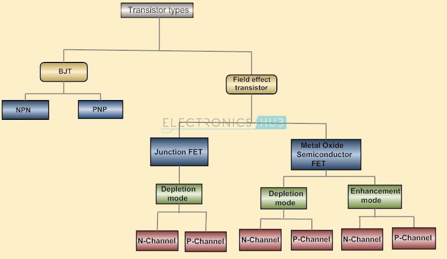
From the time of first transistor invention to present days the transistors are classified into different types depending on either construction or operation, they are explained using tree diagram as below.
Transistor Tree Diagram
The transistors classification can be understood by observing the above tree diagram. Transistors are basically classified into two types; they are Bipolar Junction Transistors (BJT) and Field Effect Transistors (FET). The BJTs are again classified into NPN and PNP transistors. The FET transistors are classified into JFET and MOSFET.
Junction FET transistors are classified into N-channel JFET and P-channel JFET depending on their function. MOSFET transistors are classified into Depletion mode and Enhancement mode. Again depletion and enhancement mode transistors are classified into N-channel JFET and P-channel.
Nowadays, the vacuum tubes are replaced with transistors because the transistors have more benefits over vacuum tubes. Transistors are small in size and it requires low voltage for operation and also it has low power dissipation. Due to these reasons the transistor is used in many applications such as amplifiers, switching circuits, oscillators and also in almost all electronic circuits.
Types of Transistors
Transistor is the proper arrangement of different semiconductor materials. General semiconductor materials used for transistor are silicon, germanium, and gallium-arsenide. Basically the transistors are classified depending on their structure. Each type of transistors has their own characteristics, advantages and disadvantages.
Some transistors are designed primarily for switching purpose, other side some are designed for amplification purpose and some transistors are designed for both amplification and switching purposes. Depending on the structure the transistors are classified into BJT and FET.
Junction Transistors
Junction transistor is generally called as Bipolar Junction Transistor (BJT). The BJT transistors have three terminals named emitter (E), Base (B), Collector (C). The name itself indicates that it has two junctions between p-type and n-type semiconductors. The BJT transistors are classified in to NPN and PNP transistors depending on the construction.
Unlike FET transistors, the BJT transistors are current-controlled devices. If small amount of current flows through the base of a BJT transistor then it causes to flow large current from emitter to collector. The BJT transistors have low input impedance and it causes to flow large current through the transistor.
The BJT transistors are only the transistors which are turned ON by the input current which is given to the base. Bipolar junction transistors can operate in three regions, they are
- Cut-off Region: Here the transistor is in ‘OFF’ state i.e the current flowing through the transistor is zero.
- Active Region: Here the transistor acts as an amplifier.
- Saturation Region: Here the transistor is in fully ‘ON’ state and also works as a closed switch.
NPN Transistor
NPN is one of the two types of Bipolar Junction Transistors (BJT). The NPN transistor consists of two n-type semiconductor materials and they are separated by a thin layer of p-type semiconductor. Here the majority charge carriers are electrons and holes are the minority charge carriers. The flowing of electrons from emitter to collector forms the current flow in the transistor through the base terminal.
A small amount of current at base terminal causes to flow large amount current from emitter to collector. Nowadays the generally used bipolar transistor is NPN transistor, because the mobility of electrons is greater than mobility of holes. The standard equation for the currents flowing in the transistor is
IE = IB + IC
The symbols and structure for NPN transistors are given below.
PNP Transistor
The PNP is another type of Bipolar Junction Transistors (BJT). The PNP transistors contain two p-type semiconductor materials and are separated by a thin layer of n-type semiconductor. The majority charge carriers in the PNP transistors are holes and electrons are minority charge carriers. The arrow in the emitter terminal of transistor indicates the flow of conventional current. In PNP transistor the current flows from Emitter to Collector.
The PNP transistor is ON when the base terminal is pulled to LOW with respect to emitter. The symbol and structure for PNP transistor is shown below.
FET (Field Effect Transistor)
The Field-Effect-Transistor (FET) is another transistors type. Basically the FET transistors have three terminals they are gate (G), Drain (D) and Source (S). FET transistors are classified into Junction Field Effect transistors (JFET) and Insulated Gate FET (IG-FET) or MOSFET transistors. For the connections in the circuit we also consider fourth terminal called base or substrate. The FET transistors have control on the size and shape of a channel between source and drain which is created by applied voltage. The FET transistors are uni-polar transistors because they perform single channel operation where as BJT transistors are bipolar junction transistors. The FET transistors have high current gain than BJT transistors.
JFET (Junction-Field Effect Transistor)
The Junction-Field-Effect transistor (JFET) is an earliest and simple type of FET transistors. These JFETs are used as switches, amplifiers and resistors. This transistor is a voltage controlled device. It doesn’t need any biasing current. The voltage applied between gate and source controls the flow of electric current between source and drain of a transistor. The JFET transistors are available in both N-channel and P-channel types.
N-Channel JFET
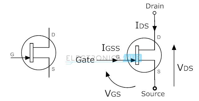
In N-channel JFET the current flow is due to the electrons. When voltage is applied between gate and source, a channel is formed between source and drain for current flow. This channel is called N-channel. Nowadays N-channel JFET transistor is most preferable type than P-channel JFET. The symbols for N-channel JFET transistor are given below.
P-Channel JFET
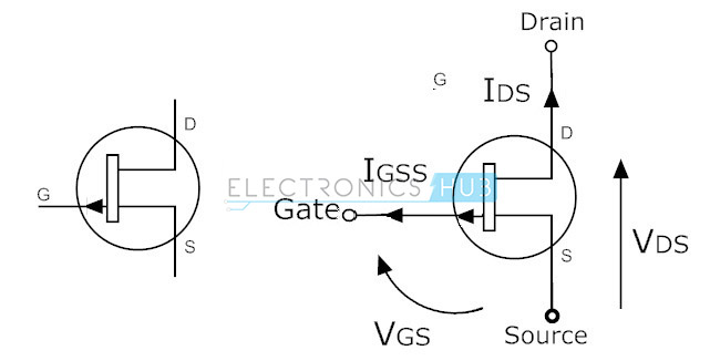
In this JFET transistor the current flow is because of holes. The channel between source and drain is called P-channel. The symbols for P-channel JFET transistors are given below. Here arrow marks indicates the direction of current flow.
MOSFET
Metal-Oxide-Semiconductor Field Effect Transistor (MOSFET) is most useful type of among all transistors. The name itself indicates that it contains metal gate terminal. The MOSFET has four terminals drain, source, gate and body or substrate (B). MOSFET has many advantages over BJT and JFET, mainly it offer high input impedance and low output impedance. It is used in low power circuits mainly in chip designing technologies.
The MOSFET transistors are available in depletion and enhancement types. Further the depletion and enhancement types are classified into N-channel and P-channel types.
N-Channel MOSFET
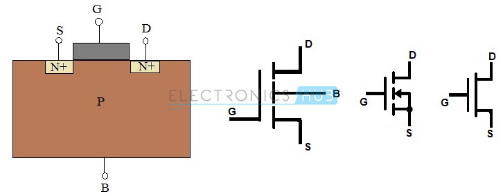
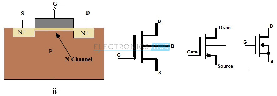
The MOSFET having N-channel region between source and drain is called N-channel MOSFET. Here the source and gate terminals are heavily doped with n-type materials and substrate is doped with p-type semiconductor material. Here the current flow between source and drain is because of electrons. The gate voltage controls the current flow in the circuit. N-channel MOSFET is most preferable than P-channel MOSFET because the mobility of electrons is high than mobility of holes. The symbols for N-channel MOSFET transistors are given below.
P- Channel MOSFET
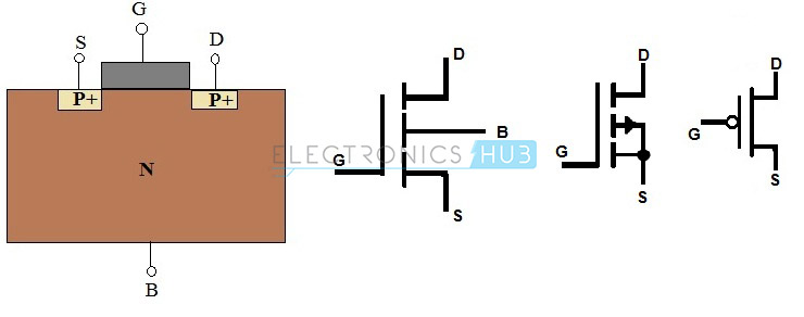
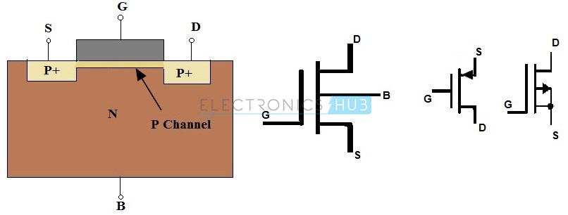
The MOSFET having P-channel region between source and drain is called as P-channel MOSFET. Here the source and drain terminals are heavily doped with P-type material and the substrate is doped with N-type material. The current flow between source and drain is because of holes concentration. The applied voltage at gate will controls the flow of current through channel region. The symbols for P-channel MOSFET transistors in depletion and enhancement types are given below.
Transistors Based on Function
Transistors are also classified depending on the functions that mean what the transistors do. Different types of transistors based on their function are explained below.
Small Signal Transistors
The basic function of small signal transistors is to amplify small signals even these transistors are used for switching purpose. Small signal transistors are available in market in the form of NPN and PNP transistors. We can see some value on the body of small signal transistor this value indicates hFE of transistor.
Depending on this hFE value we can understand the capacity of transistor to amplify the signal. The hFE values are present within the range of 10 to 500. The collector current value of these transistors is 80 to 600mA. This type of transistors operates with the frequency range of 1 to 300MHz. The name of the transistor itself indicates that these transistors amplify small signals which use small voltages and currents, such as few milli volts and milli amperes of current.
Resource link: learningaboutelectronics.com/images/Small-signal-transistor.png
Small signal transistors are used in almost all types of electronic equipments and also these transistors are used in several applications, some of them are ON or OFF switches for general use, LED diode driver, Relay driver, Audio mute function, Timer circuits, Infrared diode amplifier, Bias supply circuits etc.
Small Switching Transistors
Small switching transistors are the transistors which are primarily used for switching after that also used for amplification. Like small signal transistors, small switching transistors are also available in the form of NPN and PNP and these type of transistors are also have hFE values. The hFE value range for these transistors is from 10 to 200. At hFE value 200 the transistors are not good amplifiers even though they act as better switches. The collector current values ranges from 10 to 1000mA. These transistors are used mostly in switching applications.
Resource link: learningaboutelectronics.com/images/Small-switching-transistor.png
Power Transistors
The transistors which are used in the high power amplifiers and power supplies are called as “power amplifiers”. The collector terminal of this transistor is connected to the base of a metal device and this structure acts as heat sink which dissipates excess power for the applications.
These types of transistors are available in the form of NPN, PNP and Darlington transistors. Here the collector current values range from 1 to 100A. The operating frequency range from 1 to 100MHz. The power values of these transistors are range from 10 to 300W. The name of the transistor itself indicates that the power transistors are used in the applications where high power, high voltage and high current are required.
Resource link: learningaboutelectronics.com/images/Power-transistors.png
High Frequency Transistors
High frequency transistors are used for small signals which operate at high frequencies and these are used in high speed switching applications. High frequency transistors are also called as RF Transistors. These transistors have maximum frequency values of about 2000MHz. The collector current (IC) value ranges from 10 to 600mA. These types of transistors are also available in the form of NPN and PNP. These are mainly used in the applications of high frequency signals and also this transistors must be ON or OFF at high speeds only. These transistors are used in HF, VHF, UHF, CATV and MATV oscillator and amplifier circuits.
Resource link: learningabouelectronics.com/images/High-frequency-transistors.jpg
Photo Transistor
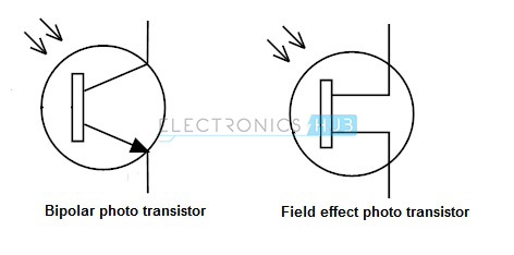
Photo transistors are the transistors which operate depending on the light that means these transistors are light sensitive. The general photo transistor is nothing but a bipolar transistor which contains light sensitive area instead of base terminal. The photo transistors have only 2 terminals instead of general 3 terminals. The transistor operates depending on the light. When the light sensitive area is dark then no current flows in transistor i.e. transistor is in OFF state.
Resource link: learningaboutelectronics.com/images/Phototransistors.jpg
When light sensitive area is exposed to light then a small amount of current generates at base terminal and it causes to flow large current from collector to emitter. The photo transistors are available in both BJT and FET transistor types. These are named as photo-BJTs and photo-FETs.
Unlike photo-BJTs, the photo-FETs are generating gate current by using light which controls the current flow between drain and source terminals. Photo-FETs are more sensitive to light than photo-BJTs. The symbols for photo-BJT and photo-FETs are shown above.
Unijunction Transistors:
Resource link: learningaboutelectronics.com/images/Unijunction-transistor.png
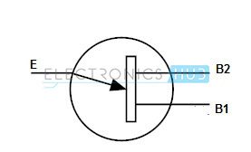
Unijunction transistors are used only as electrically controlled switches. These transistors do not contain any amplification characteristics because of their design. These are generally three lead transistors. Now we see the operation of unijunction transistor. If there is no potential difference between emitter and any one of the base terminals (B1 or B2) then a small amount of current flows between B1 and B2.
If sufficient amount of voltage is applied to the emitter terminal then high current generates at emitter terminal and it adds to small current between B1 and B2, then it causes to flow large current in the transistor. Here the emitter current is the primary current source for total current in the transistor. The current between the terminals B1 and B2 is very small, due to this reason these transistors are not suitable for amplification purpose.





0 comments
Post a Comment